CMSI 284: Welcome to Week 05
This Week's Agenda
For this week, here's the plan, Fran…
- Announcements
- Logic Components
- Gates and Truth Tables
- Combining the Parts to Make a Machine
- Quiz #1 on Thursday/Friday
Logic Components
As programmers, we have often used the boolean data type. We know well that it can have only one of two values, either true or false. That fits perfectly with the idea of binary, on or off, and with the way a digital computer works, as a series of switches. We've seen how we can represent the information of numbers and characters in the memory of a computer. But how the heck do we get those on and off states to turn into actual computation? What does the computer actually DO when adding two numbers?
The answer lies in the digital logic components from which the CPU is made. These are the working circuts that make the magic!
There are a couple of terms associated with the concepts of digital logic:
- Integrated Circuit: this is a collection of circuitry which is micro-miniaturized
so that it fits onto a single small device. Inside an
IC
there are lots of transistors, resistors, capacitors, teeny-tiny wires, all on a VERY VERY VERY small device. See the picture below. - Logic Gate: this is a concept that is used to explain how one or more parts of an IC works. It *is* actually a piece of hardware, but we visualize it by using several diagrammatic shapes. Each shape represents a specific kind of gate.
- Truth Table: this is another representation, usually in the form of a small sized table of rows and columns showing all possible input combinations, and the resulting output value for each one.
Gates and Truth Tables
There are three basic types of gates: AND, OR, and NOT.
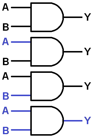
They are all made with transistors, which are like tiny on/off switches. The AND gate
circuit is set up so that only when both of the transistors are ON
will it produce an output; at
all other times [both inputs off, one on and the other off, the other on and the one off] there will be
NO OUTPUT [actually a zero
voltage level]. Here is the logic diagram symbol:
|
In the diagram, |
| AND GATE TRUTH TABLE | ||
|---|---|---|
| A | B | Y |
| 0 | 0 | 0 |
| 0 | 1 | 0 |
| 1 | 0 | 0 |
| 1 | 1 | 1 |
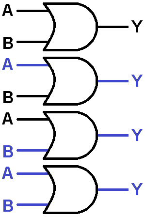
The OR gate comes next. Notice the similarity of the diagram. There are still two inputs,
|
|
| OR GATE TRUTH TABLE | ||
|---|---|---|
| A | B | Y |
| 0 | 0 | 0 |
| 0 | 1 | 1 |
| 1 | 0 | 1 |
| 1 | 1 | 1 |
|
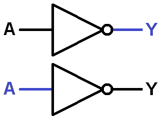
Last but not least is the NOT gate, also known as an inverter because whatever logic level appears on its input, the OPPOSITE value appears on its output. |
| NOT GATE TRUTH TABLE | |
|---|---|
| A | Y |
| 0 | 1 |
| 1 | 0 |
From these three simple gates, you can make all the parts that are required to have an entire computer! Of course, there are BILLIONS of these gates in a modern CPU, but it all boils down to the combinations of those basic circuits.
One of the first things that engineers do with gates is combine the AND and the NOT to make a special
type of gate called a NOT-AND
gate, or more commonly, a NAND gate. The idea is
to take the output of an AND gate and run it through a NOT gate. Usually a little circle is put on the
output of the AND gate to denote that it has the inverter function on the output. If you look at the
diagram above for NOT you will see that little circle, or bubble
on the output. That bubble is
what is coopted for use with the NAND gate.
You can also make a NOR gate, and by combining those three gates you can create an XOR or exclusive OR gate. You can combine those functions in other ways to make another device called a flip-flop, and other devices called adders, multiplexers, selectors, and many more. In fact, the central part of the CPU, the Arithmetic Logic Unit [ALU] is exactly that kind of composite device!
You will have a chance to study and learn the operation of these devices in more detail in your Logic Class, EE 385, later in your career here. For now, we'll be looking at ways to combine the parts using our truth table approach.
Combining the Parts to Make a Machine
First, let's look at a way to model a NAND gate using our truth tables. As you know, a NAND gate is just an AND gate with a NOT on the output. So, we can model that with the following table:
| NAND GATE TRUTH TABLE | ||||
|---|---|---|---|---|
| A | B | A 'AND' B | 'NOT' A 'AND' B | Y |
| 0 | 0 | 0 | 1 | 1 |
| 0 | 1 | 0 | 1 | 1 |
| 1 | 0 | 0 | 1 | 1 |
| 1 | 1 | 1 | 0 | 0 |
Since the Y
and the 'NOT' A 'AND' B
values are the same, we can abbreviate the table as
follows:
| NAND GATE TRUTH TABLE | |||
|---|---|---|---|
| A | B | A 'AND' B | A NAND B |
| 0 | 0 | 0 | 1 |
| 0 | 1 | 0 | 1 |
| 1 | 0 | 0 | 1 |
| 1 | 1 | 1 | 0 |
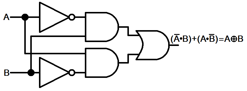
We can do similar things for tables with combinations of gates. For example, consider a device that has two inputs, A and B. Let A be the input to BOTH a NOT and an AND, but with the NOT output going as input to a SECOND AND gate. Then let B be the input to BOTH a NOT and an AND, but with the reverse of the other set up. Then let the outputs of both AND gates become the inputs to an OR gate. The output will actually end up being a XOR gate! We can then have the following truth table:
| NAND/OR GATE TRUTH TABLE | ||||||
|---|---|---|---|---|---|---|
| A | B | N | M | BN | AM | Y |
| 0 | 0 | 1 | 1 | 0 | 0 | 0 |
| 0 | 1 | 1 | 0 | 1 | 0 | 1 |
| 1 | 0 | 0 | 1 | 0 | 1 | 1 |
| 1 | 1 | 0 | 0 | 0 | 0 | 0 |
Note here for clarity, N
is the NOT of A, M
is the NOT of B, so that BN
is the AND
of B-AND-NOT-A
and AM
is the AND of A-AND-NOT-B
. TheY
output then is the
output of the OR of those two columns.
Now that you know what the table looks like, see if you can draw what the gate diagram [also known as a schematic diagram would look like. After you've given it a shot, click here to see the answer.
The next thing we need to look at is the way that computers add. It's actually much simpler than what we
are used to with normal
addition, because we only have to use two bits of input and one bit for
output. There are, of course, four possible input combinations, and four possible output combinations,
as you can see from the following table:
HALF-ADDERTRUTH TABLE | |||
|---|---|---|---|
| A | B | SUM | CARRY |
| 0 | 0 | 0 | 0 |
| 0 | 1 | 1 | 0 |
| 1 | 0 | 1 | 0 |
| 1 | 1 | 1 | 1 |
Looked at in the more traditional
format, it looks like this:
      0              0              1              1
      0              1              0              1
      --------       --------       --------       --------
      0  sum         1  sum         1  sum         0  sum
      0  carry       0  carry       0  carry       1  carry
The logic circuit for a full-adder is a little more advanced than we will delve into this week. For now, see if you can follow the logic, knowing what you now know about the gate operations. Basically, the sum output is the XOR of the inputs, and if both the inputs are ON, the AND gate generates a carry output. |
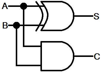
|
The various gates, both individually and collectively as combinational logic
functions, are available on Integrated Circuit [IC] chips. There are several different
families
of these.
Here is a link to the
Wikipedia page that lists and describes the 7400
family. The picture below shows
Investigation: See if you can figure out the truth tables for the following combinations of gates.
- A two-input AND gate and an INVERTER output to a single OR gate, whose output goes to an INVERTER.
- A three-input system has two of its inputs going to a two-input NAND gate. The third input and the output of the NAND gate are inputs to an AND gate.
- A three-input system as A, B, and X inputs. A and X are both inputs to an AND gate. The X input also goes to an INVERTER whose output goes with B to the other AND gate. The outputs of both the AND gates go to an OR gate.
- A NOR gate is an OR gate with an INVERTER on the output. Use a truth table to determine if this is the same thing as an AND gate in terms of its outputs
Week Five Wrap-up
That's probably enough for the this week. Be sure to check out the links on this page. Try to figure out a few truth tables for combinations of gates. Don't forget the test on Thursday/Friday!
